SEM
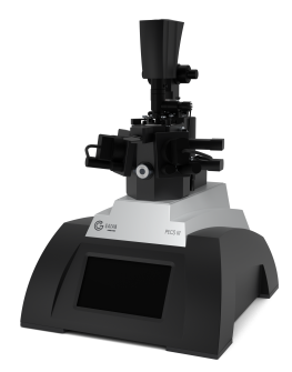
PECS III System
Designed to produce consistent, high-quality surfaces across semiconductors, batteries, and advanced materials using a single, integrated workflow.
Advantages
The PECS™ III is a broad-beam argon ion milling system designed to produce consistent, high-quality surfaces across semiconductors, batteries, and advanced materials using a single, integrated workflow. It enables reliable surface preparation for complex, multi-material samples while minimizing operator dependence and preparation-induced artifacts.
Consistent, high quality surfaces: Produces uniform, low damage surfaces suitable for demanding analytical techniques across a wide range of materials.
High throughput for complex materials: Improves milling rates by 4.4x and enables preparation of larger areas for faster, more meaningful results.
Up to 7x wider cross-section capability: Prepares large area cross-sections with ease, supporting semiconductor, battery, and multilayer systems.
Universal, simple preparation across diverse materials: Ensures predictable, repeatable outcomes independent of operator skill, reducing rework and preparation variability.
Streamlined workflow: Delivers results using one preparation workflow, reducing handling steps and improving overall efficiency.
Integrated coating functionality: Deposits consistently thin coatings to protect sample surfaces and enable analysis of delicate and non-conductive materials.